Industry Challenges
The Fastest Way to Verify the Physical Layer on Your PCI Express (PCIe) Link
![]() 8 min
8 min
![]() 7 min
7 min

As data rates continuously increase and system architectures become more complex across all modern technology, it is crucial for engineers to better understand jitter transfer functions to help them design, optimize, and troubleshoot systems that meet strict performance requirements. In this article, discover how we use Introspect’s SV1C Personalized SerDes Tester to rapidly develop and execute phase-locked loop (PLL) jitter transfer function measurement. We leverage the integrated nature of the tool and its automation features to develop tests, execute scripts, and generate automatic reports in minutes.
We will first define jitter transfer and its relevance to high-speed standards. Then, we describe the measurement concept used in this article and construct a very simple Pinetree test procedure for the automatic collection of PLL jitter transfer functions and loop bandwidth parameters. Finally, we describe advanced topics related to min-max VCO testing, time-domain testing, and linearity.
As can be seen in the PCI Express example below (Figure 1), multiple phase-locked loop (PLL) circuits exist in both the transmitter and the receiver. These circuits are critical in order to ensure error-free operation at very high data rates (e.g. 32 Gbps) while using relatively inexpensive clocking topologies. When viewed in the “phase domain”, these phase-locked loops essentially behave as frequency selective filters (H1, H2, and H3 in the figure), passing certain frequency bands of “phase” and rejecting other frequency bands.
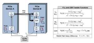
Strictly speaking, PLLs are nonlinear filter systems; however, it is possible to model their behavior as linear transfer functions as shown in Figure 1. The theory behind these transfer functions is somewhat complex and the significant point in this article is that parameters such as ωn and ζ are critical to the operation of digital SerDes links at multi-Gbps speeds. For example, having too much peaking (as affected by ζ) or having a large mismatch in ωn between transmitters and receivers can have a catastrophic effect on link BER performance.
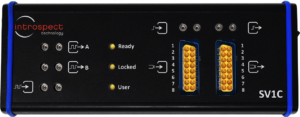
To perform jitter transfer measurement, we used the SV1C Personalized SerDes Tester. The SV1C is ideal for this purpose because it includes high precision calibrated jitter injection sources, and it contains parallel jitter measurement channels and post-processing engines. The integration of all of these functions in an instrument form factor that fits in the palm of one hand affords great flexibility in analyzing multiple transfer functions in complex links such as the ones shown in Figure 1.
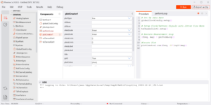
Specifically, and referring to Figure 3, the SV1C is used to automatically execute the following sequence of steps shown in the figure. First, calibrated sine wave jitter waveforms are generated as a stimulus to the PLL under test or CDR under test. Then, the PLL response to the sinusoidal input is measured. This response is itself generally sinusoidal in nature as well, although its amplitude and phase will depend on the frequency-selective nature of the PLL under test. Finally, Pinetree automatically analyzes the output and input sine waves collectively in the frequency domain, performs the automated sweep across the target frequency range, and constructs the desired result.
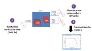
The concept of Figure 3 is extremely simple, and it is enabled by the automation tools in Pinetree and by the availability of versatile calibrated jitter sources in the SV1C. Specifically, the jitter being generated from the SV1C is already self-calibrated.
Thus, when it is used to measure the response of a PLL, the tool already knows what the PLL input jitter waveform looks like, which results in significant time savings: in the past, one had to measure the jitter injection source first using, say, an oscilloscope before applying this jitter to the PLL and measuring its output using the same oscilloscope.
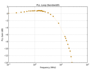
The results of executing the test procedure of Figure 4 are described in this section. Figure 5 shows the entire transfer function for a single PLL that was measured. This graph was generated automatically after execution of the test procedure. As can be seen, a low pass function is observed with a 3dB frequency of about 9 MHz. We also see that there is about 1 dB of peaking around the frequency of 2 MHz.
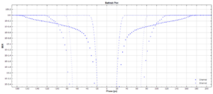
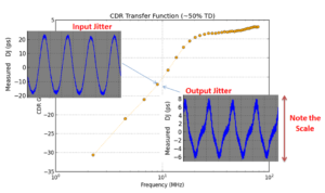
It is important to note that each solid circle in the graph of Figure 5 is an explicit execution of the sinusoidal input/output sequence described in Figure 3. To illustrate this, we show bathtub plots in Figure 6 for both the input and output signals of the PLL at one iteration in the loop. The input signal has a very wide jitter lobe that is typical of sinusoidal jitter; on the other hand, the output of the PLL has a much narrower lobe because the jitter is largely attenuated by the PLL at that particular frequency. The test procedure simply analyzed results such as these for all points on the graph of Figure 5.
With the basic transfer function collection process described, we can now proceed to performing much more elaborate characterization steps with the SV1C on other devices under test.
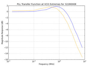
In Figure 7, we show the result of testing another device across its VCO frequency range. The figure shows two transfer functions, one at the minimum VCO frequency and one at the maximum VCO frequency. Both bandwidth and peaking are altered slightly as is typical of ring oscillator PLLs. This figure was obtained by creating an outer loop to the test procedure from Figure 4 in which the globalClockConfig.setup() component was iterated on to generate stimulus signals at different frequency values.
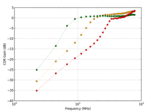
In Figure 8, a CDR frequency response is illustrated. The transfer function is now a high-pass function as shown by the large attenuation at low frequencies and low attenuation at high frequencies. Finally, Figure 9 shows a parallel measurement in which three traces are collected simultaneously.
In this article, we used the SV1C to perform rapid and highly flexible jitter transfer testing on PLLs and CDR circuits. You may also use the SV2C Personalized SerDes Tester for this exact test. We described the importance of jitter transfer testing, the measurement concept deployed, and simple test procedures for data collection. We also showed advanced analysis topics including time-domain measurement and parallel measurement.
We’re always happy to chat about all things jitter transfer functions. To keep the conversation going, send us an email at info@introspect.ca.


