
Industry Challenges
Protocol Analyzer or Oscilloscope?
![]() 8 min
8 min
![]() 9 min
9 min


Introspect Technology’s tools are currently being used to develop and test semiconductor components that are powering the metaverse, and we’re already seeing some interesting trends! While most articles about the metaverse often focus on the end-use applications, we, on the other hand, are keenly interested in how the technology underpinnings of components and systems enabling the metaverse will look like in the future. Read on to learn more about our involvement in metaverse technology and the insights that we have gained so far. Most importantly, learn more about our most popular tools that are used by leading-edge metaverse pioneers in the technology industry.
In simple terms, the metaverse is a future version of the internet in which there are many more ways by which humans interact with the virtual world. More importantly, it is a future in which our senses are stimulated in a hybrid manner through both real-world and virtual-world inputs. For example, when we drive a car that has a head-up display (HUD), we are experiencing inputs from the real world (the real road ahead) and from a display that overlays virtual data on top of the real-world scene we are seeing. This is an example of a hybrid-reality, augmented reality, or extended-reality application that already exists today, and the metaverse promises to make such an application a lot more nuanced and seamless.
When it comes to making chips that power these extended-reality and/or virtual-reality experiences, design engineers are faced with unprecedented challenges related to integration and performance. On one hand, the chips must be really tiny if they are to be placed on, say, a human eye, and on the other hand, they must enable immersive experiences which require a great deal of computing power. These are exciting challenges, and they explain why achieving the metaverse promise requires massive investment from the entire industry. The following sections articulate some of these challenges, especially in the context of design-for-testability (DFT).
Typical interfaces that are used in extended- and virtual-reality applications include display and camera interfaces like those specified by the MIPI® Alliance. While such interfaces are unidirectional multi-Gbps links, conventional instantiations of these interfaces sometimes include an internal design-for-test option that enables loopback. This makes testing during manufacturing easier because a transmitter under test can be looped back to a “dummy” receiver or a receiver under test can be stimulated by a “dummy” transmitter. However, with the increased pressure on integration that is created by new metaverse applications, the cost of such loopback connections is prohibitive. Designers are often pushed to extreme limits of package miniaturization and the elimination of any unnecessary pads. This is counter to what a loopback connection entails. So, expect more DFT strategies that rely more on creative test modes and less on loopback!
When debugging a system during design validation, different prototype boards can be used by engineers. For example, in older smart phone applications, a “blown-up” phone PCB was often used, which had electrical connections that were similar to the final phone formfactor but that were spaced out for easier probing access. More and more, we are seeing that such a blown-up PCB approach is not sufficient for complete debugging and that “formfactor” probing is necessary. That is, engineers now have to probe the final formfactor of the product that they are developing, and this is increasingly challenging. Figure 1 shows an example of formfactor probing where a device is being debugged for subtle protocol faults.
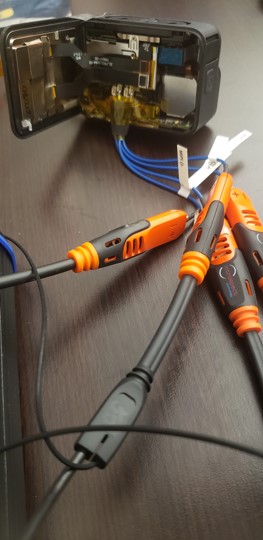
Figure 1: Illustration of formfactor probing
A topic that is closely related to the metaverse is ambient computing where the environment reacts to the content that we are producing or consuming. An example that is present in our current generation of technology is smart lighting controls that are synchronized with video or audio. Referring to Figure 2 below, notice how the ambient light around the TV reflects the currently displayed colors within the TV.

Figure 2: Example of ambient computing — wall lighting is synchronized with video on the TV.
The above example is only a conceptual illustration, but there are many extended-reality applications that require high bandwidth transmissions between devices, often wirelessly. Sensors must now generate millions of samples per second as opposed to tens of samples per second. This is why interfaces such as the MIPI I3C® bus interface are such a big deal in future metaverse applications.
Almost every high-speed interface that our tools cover will have an application in the metaverse, whether directly through the development of wearable devices or indirectly through the development of data center and communications technology infrastructures for powering the metaverse’s backend. For the purposes of this article, we highlight a couple of solutions.
Our generator products cover a wide range of applications ranging from pre-silicon prototyping to post-silicon characterization, to design validation, and finally to mass production testing. Explore the C Series products for bench applications and the E Series products for mass production testing.
![]()
Figure 3: Our MIPI generators are used for characterization, debug, and production testing.
Our analyzer products have become indispensable for characterization and for detailed protocol debug. They are also used for innovating applications such as system-level characterization and mass production testing.
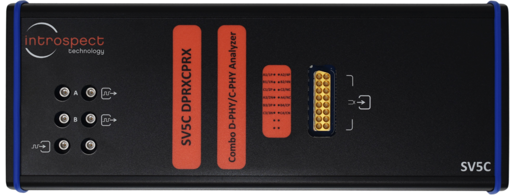
Figure 4: Our MIPI analyzers are used for characterization, debug, and production testing.
Our world-renowned SV4E-I3C has been helping customers develop and debug I3C applications for almost 5 years now. It keeps evolving with the industry and keeps adding incredibly powerful features. Stay tuned for some stunning announcements on this product!
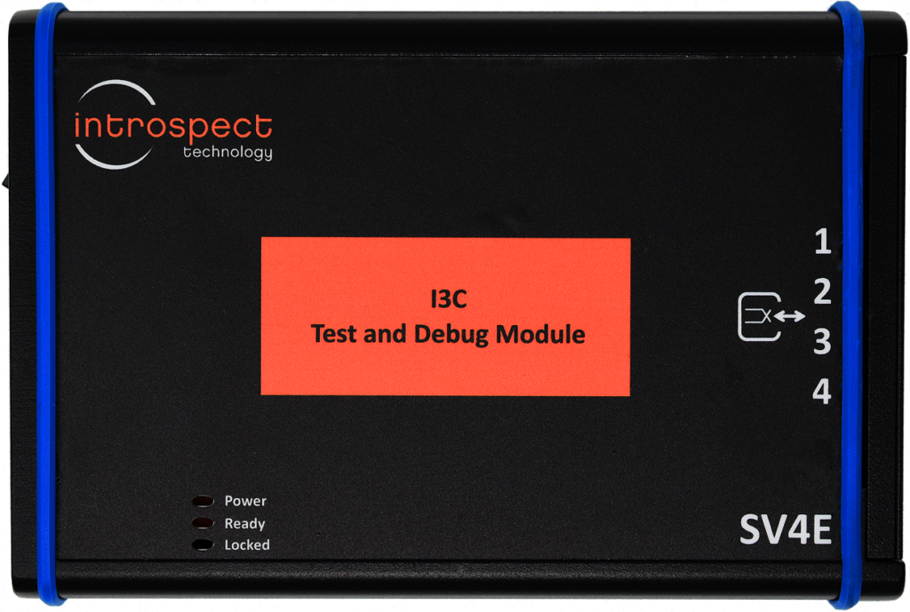
Figure 5: Our I3C solution enables exercising, analyzing, and high volume testing.
Metaverse development is well under way, and it has been for a while. It creates tremendous new challenges and opportunities, and Introspect’s tools are able to help the world’s brightest engineers overcome these challenges!
[1] Technology photo created by rawpixel.com – www.freepik.com
